Safety Summary
Safety Depends On You
The following general safety precautions must be observed during all phases of operation, service, and
repair of this equipment. Failure to comply with these precautions or with specific warnings elsewhere in
this manual violates safety standards of design, manufacture, and intended use of the equipment.
Motorola, Inc. assumes no liability for the customer’s failure to comply with these requirements.
The safety precautions listed below represent warnings of certain dangers of which Motorola is aware. You,
as the user of the product, should follow these warnings and all other safety precautions necessary for the
safe operation of the equipment in your operating environment.
Ground the Instrument.
To minimize shock hazard, the equipment chassis and enclosure must be connected to an electrical ground.
The equipment is supplied with a three-conductor ac power cable. The power cable must be plugged into
an approved three-contact electrical outlet. The power jack and mating plug of the power cable meet
International Electrotechnical Commission (IEC) safety standards.
Do Not Operate in an Explosive Atmosphere.
Do not operate the equipment in the presence of flammable gases or fumes. Operation of any electrical
equipment in such an environment constitutes a definite safety hazard.
Keep Away From Live Circuits.
Operating personnel must not remove equipment covers. Only Factory Authorized Service Personnel or
other qualified maintenance personnel may remove equipment covers for internal subassembly or
component replacement or any internal adjustment. Do not replace components with power cable
connected. Under certain conditions, dangerous voltages may exist even with the power cable removed. To
avoid injuries, always disconnect power and discharge circuits before touching them.
Do Not Service or Adjust Alone.
Do not attempt internal service or adjustment unless another person capable of rendering first aid and
resuscitation is present.
Use Caution When Exposing or Handling the CRT.
Breakage of the Cathode-Ray Tube (CRT) causes a high-velocity scattering of glass fragments (implosion).
To prevent CRT implosion, avoid rough handling or jarring of the equipment. Handling of the CRT should
be done only by qualified maintenance personnel using approved safety mask and gloves.
Do Not Substitute Parts or Modify Equipment.
Because of the danger of introducing additional hazards, do not install substitute parts or perform any
unauthorized modification of the equipment. Contact your local Motorola representative for service and
repair to ensure that safety features are maintained.
Dangerous Procedure Warnings.
Warnings, such as the example below, precede potentially dangerous procedures throughout this manual.
Instructions contained in the warnings must be followed. You should also employ all other safety
precautions which you deem necessary for the operation of the equipment in your operating environment.
!
WARNING
Dangerous voltages, capable of causing death, are
present in this equipment. Use extreme caution when
handling, testing, and adjusting.
All Motorola PWBs (printed wiring boards) are manufactured by UL-recognized
manufacturers, with a flammability rating of 94V-0.
!
WARNING
This equipment generates, uses, and can radiate electromagnetic energy. It may cause or be susceptible to
electro-magnetic interference (EMI) if not installed and
used in a cabinet with adequate EMI protection.
The computer programs stored in the Read Only Memory of this device contain
material copyrighted by Motorola Inc., 1995, and may be used only under a license
such as those contained in Motorola’s software licenses.
Motorola® and the Motorola symbol are registered trademarks of Motorola, Inc.
All other products mentioned in this document are trademarks or registered
trademarks of their respective holders.
©Copyright Motorola 1997
All Rights Reserved
Printed in the United States of America
This Chapter Covers
❏ Details about this manual
❏ Terminology, conventions, and definitions used
❏ Other publications relevant to the MVME187
About this Manual
This manual supports the setup, installation, and debugging of the
RISC-based MVME187 Single Board Computer; a highperformance engine for VMEbus-based low- and mid-range OEM
and integrated systems, embedded controllers, and other singleboard computer applications.
This manual provides:
❏ A general Board Level Hardware Description in Chapter 2
❏ Hardware Preparation and Installation instructions in Chapter 3
❏ Debugger General Information in Chapter 4
❏ Debugger/monitor commands, and other information about
Using the 187Bug Debugger in Chapter 5
❏ Other information needed for start-up and troubleshooting of
the MVME187 RISC Single Board Computer, including
– Configure and Environment Commands in Appendix A
– Disk/Tape Controller Data in Appendix B for controller
modules supported by 187Bug
– Network Controller Data in Appendix C
– Procedures for Troubleshooting CPU Boards in Appendix D
– EIA-232-D Interconnections in Appendix E
Terminology, Conventions, and Definitions
Used in this Manual
Data and Address Parameter Numeric Formats
Throughout this manual, a character identifying the numeric
format precedes data and address parameters as follows:
For example, “12” is the decimal number twelve, and “$12” is the
decimal number eighteen.
Unless otherwise specified, all address references are in
hexadecimal.
Signal Name Conventions
An asterisk (*) follows signal names for signals which are level or
edge significant:
$ dollar specifies a hexadecimal character
% percent specifies a binary number
& ampersand specifies a decimal number
Term * Indicates
level
significant The signal is true or valid when the signal is low.
edge
significant
The actions initiated by that signal occur on high
to low transition.
Assertion and Negation Conventions
Assertion and negation are used to specify forcing a signal to a
particular state. These terms are used independently of the voltage
level (high or low) that they represent.
Data and Address Size Definitions
Data and address sizes are defined as follows:
Big-Endian Byte Ordering
This manual assumes that the MPU on the MVME187 always
programs the CMMUs with big-endian byte ordering, as shown
below. Any attempt to use little-endian byte ordering will
immediately render the MVME187Bug debugger unusable.
Term Indicates
Assertion and assert The signal is active or true.
Negation and negate The signal is inactive or false.
Name Size Numbered Significance Called
Byte 8 bits 0 through 7
bit 0 is the
least
significant
Two-byte 16 bits 0 through 15
bit 0 is the
least
significant
halfword
Four-byte 32 bits 0 through 31
bit 0 is the
least
significant
word
BIT BIT
31 24 23 16 15 08 07 00
ADR0 ADR1 ADR2 ADR3
Control and Status Bit Definitions
The terms control bit and status bit are used extensively in this
document to describe certain bits in registers.
❏ The status bit can be read by software to determine
operational or exception conditions.
True/False Bit State Definitions
True and False indicate whether a bit enables or disables the
function it controls:
Bit Value Descriptions
In all tables, the terms 0 and 1 are used to describe the actual value
that should be written to the bit, or the value that it yields when
read.
Term Describes
Control bit The bit can be set and cleared under software
control.
Status bit The bit reflects a specific condition.
Term Indicates
True Enables the function it controls.
False Disables the function it controls.
Related Documentation
The MVME187 ships with a start-up installation guide
(MVME187IG/D, the document you are presently reading) which
includes installation instructions, jumper configuration
information, memory maps, debugger/monitor commands, and
any other information needed for start-up of the board.
If you wish to develop your own applications or need more detailed
information about your MVME187 Single Board Computer, you
may purchase the additional documentation (listed on the
following pages) through your local Motorola sales office.
If any supplements have been issued for a manual or guide, they
will be furnished along with the particular document. Each
Motorola Computer Group manual publication number is suffixed
with characters which represent the revision level of the document,
such as “/D2” (the second revision of a manual); a supplement
bears the same number as a manual but has a suffix such as
“/D2A1” (the first supplement to the second edition of the
manual).
Document Set for MVME187-0xx Board
You may order the manuals in this list individually or as a set. The
manual set 68-M187SET includes:
Motorola
Publication Number Description
MVME187/D MVME187 RISC Single Board Computer User’s Manual
88KBUG1/D
88KBUG2/D
Debugging Package for Motorola 88K RISC CPUs User’s
Manual (Parts 1 and 2)
MVME187BUG MVME187Bug Debugging Package User’s Manual
VMESBCA1/PG
VMESBCA2/PG
Single Board Computer Programmer’s Reference Guide
(Parts 1 and 2)
Introduction to the MVME187 Installation Guide 1
Additional Manuals for this Board
Also available but not included in the set:
Other Applicable Motorola Publications
The following publications are applicable to the MVME187 and
may provide additional helpful information. They may be
purchased through your local Motorola sales office.
SBCSCSI/D Single Board Computers SCSI Software User’s Manual
Motorola
Publication Number Description
MVME187IG/D MVME187 RISC Single Board Computer Installation
Guide (this manual)
SIMVME187/D MVME187 RISC Single Board Computer Support
Information
The SIMVME187 manual contains the connector
interconnect signal information, parts lists, and the
schematics for the MVME187.
Motorola
Publication Number Description
MVME712M MVME712M Transition Module and P2 Adapter
Board User’s Manual
MVME712A MVME712-12, MVME712-13, MVME712A,
MVME712AM, and MVME712B Transition Modules
and LCP2 Adapter Board User’s Manual
Motorola
Publication Number Description
MC88100UM MC88100 RISC Microprocessor User’s Manual
MC88200UM MC88200 Cache/Memory Management Unit
(CMMU) User’s Manual
MC88204 MC88204 64K-Byte Cache/Memory Management
Unit (CMMU) data sheet A
Non-Motorola Peripheral Controllers Publications Bundle For your convenience, we have collected user’s manuals for each of the peripheral controllers used on the MVME187 from the suppliers. This bundle, which can be ordered as part number 68- 1X7DS, includes the following manuals
Part Number Description
NCR53C710DM NCR 53C710 SCSI I/O Processor Data Manual
NCR53C710PG NCR 53C710 SCSI I/O Processor Programmer’s Guide
CL-CD2400/2401 Cirrus Logic CD2401 Serial Controller User’s Manual
UM95SCC0100 Zilog Z85230 Serial Communications Controller
User’s Manual
290218 Intel Networking Components Data Manual
290435 Intel i28F008 Flash Memory Data Sheet
290245 Intel i28F020 Flash Memory Data Sheet
292095 Intel i28F008SA Software Drivers Application Note
292099 Intel i28F008SA Automation and Algorithms
Application Note
Part Number Description
MK48T08/18B SGS-THOMSON MK48T08 Time Clock/NVRAM
Data Sheet
MC68230/D MC68230 Parallel Interface Timer (PI/T) Data Sheet
SBCCOMPS/L Customer Letter for Component Alternatives
Applicable Non-Motorola Publications
The following non-Motorola publications are also available from
the sources indicated.
Document Title Source
Versatile Backplane Bus: VMEbus,
ANSI/IEEE Std 1014-1987
(VMEbus Specification) (This is also
Microprocessor System Bus for 1 to 4 Byte
Data, IEC 821 BUS)
The Institute of Electrical and
Electronics Engineers, Inc.
345 East 47th St.
New York, NY 10017
Bureau Central de la Commission
Electrotechnique Internationale
3, rue de Varembé
Geneva, Switzerland
ANSI Small Computer System Interface-2
(SCSI-2), Draft Document X3.131-198X,
Revision 10c
Global Engineering Documents
15 Inverness Way East
Englewood, CO 80112-5704
CL-CD2400/2401 Four-Channel MultiProtocol Communications Controller Data
Sheet, order number 542400-003
Cirrus Logic, Inc.
3100 West Warren Ave.
Fremont, CA 94538
82596CA Local Area Network Coprocessor
Data Sheet, order number 290218; and
82596 User’s Manual, order number 296853
Intel Corporation, Literature Sales
P.O. Box 58130
Santa Clara, CA 95052-8130
NCR 53C710 SCSI I/O Processor Data
Manual, order number NCR53C710DM
NCR Corporation
Microelectronics Products Division
1635 Aeroplaza Dr.
Colorado Springs, CO 80916 NCR 53C710 SCSI I/O Processor
Programmer’s Guide, order number
NCR53C710PG
MK48T08(B) Timekeeper TM and 8Kx8
Zeropower TM RAM data sheet in Static
RAMs Databook, order number DBSRAM71
SGS-THOMSON Microelectronics
Group
Marketing Headquarters
1000 East Bell Rd.
Phoenix, AZ 85022-2699
2Board Level Hardware
Description
This Chapter Covers
❏ A general description of the MVME187 RISC Single Board
Computer
❏ Features and specifications
❏ A board-level hardware overview
❏ A detailed hardware functional description, including front
panel switches and indicators
❏ Memory maps
General Description
The MVME187 is a high functionality VMEbus RISC single board
computer designed around the M88000 chip set. It features:
❏ Onboard memory expansion mezzanine module with
4, 8, 16, 32, 64 or 128MB of onboard DRAM
❏ SCSI bus interface with DMA
❏ Four serial ports with EIA-232-D interface
❏ Centronics (parallel) printer port
❏ Ethernet transceiver interface with DMA
❏ 187Bug debug monitor firmware
Onboard Memory Mezzanine Module
The MVME187 onboard DRAM mezzanine boards are available in
different sizes and with programmable parity protection or Error
Checking and Correction (ECC) protection.
❏ The main board and a single mezzanine board together take
one slot.
❏ Motorola software supports mixed parity and ECC memory
boards on the same main board.
❏ Mezzanine board sizes are 4, 8, 16, or 32 MB (parity), or 4, 8,
16, 32, 64, or 128 MB (ECC);
– Two mezzanine boards may be stacked to provide 256MB
of onboard RAM (ECC) or 64 MB (parity). The stacked
configuration requires two VMEbus slots.
❏ The DRAM is four-way interleaved to efficiently support
cache burst cycles.
❏ The parity mezzanines are only supported on 25 MHz main
boards.
A functional description of the Onboard DRAM starts on page 2-15.
SCSI Mass Storage Interface
The MVME187 provides for mass storage subsystems through the
industry-standard SCSI bus. These subsystems may include
❏ Hard and floppy disk drives
❏ Streaming tape drives
❏ Other mass storage devices.
A functional description of the SCSI Interface starts on page 2-22.
Serial Ports
The serial ports support standard baud rates of 110 to 38.4K baud.
All four serial ports use EIA-232-D drivers and receivers located on
the main board, and all the signal lines are routed to the I/O
connector.
A functional description of the Serial Port Interface starts on page
2-18.
Parallel (Printer) Port
The 8-bit bidirectional parallel port may be used as a Centronicscompatible parallel printer port or as a general parallel I/O port.
A functional description of the Parallel Port Interface starts on page
2-20.
Ethernet Transceiver Interface
The Ethernet transceiver interface is located on the MVME187, and
the industry standard connector is located on the MVME712X
transition module.
A functional description of the Ethernet Interface starts on page
2-21.
Serial
Port Function Synchronous/
Asynchronous Signals Bit Rates
1 Minimum Asynchronous RXD, CTS, TXD, and RTS
2
and
3
Full Asynchronous RXD, CTS, DCD, TXD, RTS,
and DTR
4 Full Both RXD, CTS, DCD, TXD, RTS,
and DTR
Synchronous up
to 64 k bits per
second
187Bug Firmware
The MVME187Bug debug monitor firmware (187Bug) is provided
in two of the four EPROM sockets on the MVME187.
It provides:
❏ Over 50 debug commands
❏ Up/down load commands
❏ Disk bootstrap load commands
❏ A full set of onboard diagnostics
❏ A one-line assembler/disassembler
The 187Bug user interface accepts commands from the system
console terminal.
187Bug can also operate in a System Mode, which includes choices
from a service menu.
Features
❏ M88000 Microprocessor (one MC88100 MPU and two
MC88200 or MC88204 CMMUs)
❏ 4/8/16/32/64MB of 32-bit DRAM with parity or
4/8/16/32/64/128/256MB of 32-bit DRAM with ECC
protection
❏ Four 44-pin PLCC ROM sockets (organized as two banks of
32 bits)
❏ 128KB Static RAM (with optional battery backup as a factory
build special request)
❏ Status LEDs for FAIL, STAT, RUN, SCON, LAN, +12V (LAN
power), SCSI, and VME.
❏ 8K by 8 static RAM and time of day clock with battery backup
❏ RESET and ABORT switches
❏ Four 32-bit tick timers for periodic interrupts
❏ Watchdog timer
❏ Eight software interrupts
❏ I/O
– SCSI Bus interface with DMA
– Four serial ports with EIA-232-D buffers with DMA
– Centronics printer port
– Ethernet transceiver interface with DMA
❏ VMEbus interface
– VMEbus system controller functions
– VMEbus interface to local bus (A24/A32, D8/D16/D32
and D8/D16/D32/D64BLT) (BLT = Block Transfer)
– Local bus to VMEbus interface (A16/A24/A32,
D8/D16/D32)
– VMEbus interrupter
– VMEbus interrupt handler
– Global CSR for interprocessor communications
– DMA for fast local memory – VMEbus transfers
(A16/A24/A32, D16/D32 and D16/D32/D64BLT)
Specifications
Conformance to Requirements
These boards are designed to conform to the requirements of the
following specifications:
❏ VMEbus Specification (IEEE 1014-87)
❏ EIA-232-D Serial Interface Specification, EIA
❏ SCSI Specification
Table 2-1. MVME187 General Specifications
Characteristics Specifications
Power requirements
(with all four EPROM sockets
populated and excluding
external LAN transceiver)
+5 Vdc (+/-5%) 3.5 A (typical), 4.5 A (maximum)
(at 25 MHz, with 32MB parity DRAM)
5.0 A (typical), 6.5 A (maximum)
(at 33 MHz, with 128MB ECC DRAM)
+12 Vdc (+/-5%) 100 mA (maximum)
(1.0 A (maximum) with offboard LAN
transceiver)
-12 Vdc (+/- 5%) 100 mA (maximum)
Operating temperature 0˚ to 55˚ C at point of entry of forced air
(approximately 490 LFM)
Storage temperature -40˚ to +85˚ C
Relative humidity 5% to 90% (non-condensing)
Physical
dimensions
Double-high
VMEboard
PC board with
mezzanine
module only
Height 9.187 inches (233.35 mm)
Depth 6.299 inches (160.00 mm)
Thickness 0.662 inches (16.77 mm)
PC board with
connectors and
front panel
Height 10.309 inches (261.85 mm)
Depth 7.4 inches (188 mm)
Thickness 0.80 inches (20.32 mm)
Board Level Overview
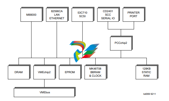
Connectors
The MVME187 has two 96-position DIN connectors: P1 and P2.
❏ P1 rows A, B, C, and P2 row B provide the VMEbus
interconnection.
❏ P2 rows A and C provide the connection to the SCSI bus,
serial ports, Ethernet, and printer.
Adapters
I/O on the MVME187 is connected to the VMEbus P2 connector.
The main board is connected to the transition modules through a P2
adapter board and cables.
Transition Modules
MVME712X transition modules provide configuration headers and
provide industry standard connectors for the I/O devices. Refer to
Figure 3-3 on page 3-22.
❏ The MVME187 supports the transition modules MVME712-
12, MVME712-13, MVME712M, MVME712A, MVME712AM,
and MVME712B (referred to in this manual as MVME712X,
unless separately specified).
Transition modules and adapter boards are covered in
MVME712M, Transition Module and P2 Adapter Board User’s Manual,
and MVME712A, MVME712-12, MVME712-13, MVME712A,
MVME712AM, and MVME712B Transition Modules and LCP2
Adapter Board User’s Manual.
ASICs
The MVME187 board features several Application Specific
Integrated Circuits (ASICs) including:
❏ VMEchip2
❏ PCCchip2
❏ MEMC040
❏ MCECC
All programmable registers in the MVME187 that reside in ASICs
are covered in the Single Board Computers Programmer’s Reference
Guide.
VMEchip2 ASIC
Provides the VMEbus interface. The VMEchip2 includes:
❏ Two tick timers
❏ Watchdog timer
❏ Programmable map decoders for the master and slave
interfaces, and a VMEbus to/from local bus DMA controller
❏ VMEbus to/from local bus non-DMA programmed access
interface
❏ VMEbus interrupter
❏ VMEbus system controller
❏ VMEbus interrupt handler
❏ VMEbus requester
PCCchip2 ASIC
The PCCchip2 ASIC provides two tick timers and the interface to
the:
❏ LAN chip
❏ SCSI chip
❏ Serial port chip
❏ Printer port
❏ BBRAM
Table 2-2. Bus Transfers
Transfer type Can be…
Processor-to-VMEbus D8, D16, or D32
VMEchip2 DMA to the
VMEbus
D16, D32, D16/BLT,
D32/BLT, or D64/MBLT
Leave a comment
Your email address will not be published. Required fields are marked *