About this Manual
Overview of Contents
This manual is divided into the following chapters and appendices:
Chapter 1, Hardware Preparation and Installation, provides MVME5500 board preparation and
installation instructions for both the board and accessories. Also included are the power-up
procedure.
Chapter 2, Functional Description, describes the MVME5500 on a block diagram level.
Chapter 3, RAM55006E Memory Expansion Module, provides a description of the RAM5500
memory expansion module, as well as installation instructions and connector pin assignments.
Chapter 4, MOTLoad Firmware, describes the basic features of the MOTLoad firmware
product.
Chapter 5, Connector Pin Assignments, provides pin assignments for various headers and
connectors on the MMVE5500 single-board computer.
Appendix A, Specifications, provides power requirements and environmental specifications.
Appendix B, Thermal Validation, provides information to conduct thermal evaluations and
identifies thermally significant components along with their maximum allowable operating
temperatures.
Appendix C, Related Documentation, provides a listing of related Emerson manuals, vendor
documentation, and industry specifications.
The MVME55006E Single-Board Computer Installation and Use manual provides the
information you will need to install and configure your MVME55006E single-board computer. It
provides specific preparation and installation information, and data applicable to the board. The
MVME55006E single-board computer will hereafter be referred to as the MVME5500.
As of the printing date of this manual, the MVME5500 supports the models listed below.
Model Number Description
MVME55006E-0161 1 GHz MPC7457 processor, 512MB SDRAM, Scanbe handles
MVME55006E-0163 1 GHz MPC7457 processor, 512MB SDRAM, IEEE handles
RAM55006E-007 Memory expansion, 512MB SDRAM
IPMC7126E-002 Multifunction rear I/O PMC module; 8-bit SCSI, Ultra Wide SCSI, one
parallel port, three async and one sync/async serial ports.
MVME712M6E Transition module with one DB-25 sync/async serial port, three DB-25
async serial port, one AUI connector, one D-36 parallel port and one 50-
pin 8-bit SCSI; includes 3-row DIN P2 adapter board and cable.
Model Number Description
MVME7616E-001 Multifunction rear I/O PMC module; 8-bit SCSI, one parallel port, two
async and two sync/async serial ports. Transition module with two DB-9
async serial port connectors, two HD-26 sync/async serial port
connectors, one HD-36 parallel port connector, one RJ-45 10/100 Ethernet
connector; includes 3-row DIN P2 adapter board and cable (for 8-bit
SCSI).
MVME7616E-011 Transition module with two DB-9 async serial port connectors, two HD-26
sync/async serial port connectors, one HD-36 parallel port connector, one
RJ-45 10/100 Ethernet connector; includes 5-row DIN P2 adapter board
and cable (for 16-bit SCSI); requires backplane with 5-row DIN
connectors.
PMCSPAN26E-002 Primary PMCSPAN with original VME IEEE ejector handles.
PMCSPAN26E-010 Secondary PMCSPAN with original VME IEEE ejector handles.
PMCSPAN16E-002 Primary PMCSPAN with Scanbe ejector handles.
PMCSPAN16E-010 Secondary PMCSPAN with Scanbe ejector handles.
The following table describes the conventions used throughout this manual.
MVME7616E-001 Multifunction rear I/O PMC module; 8-bit SCSI, one parallel port, two
async and two sync/async serial ports. Transition module with two DB-9
async serial port connectors, two HD-26 sync/async serial port
connectors, one HD-36 parallel port connector, one RJ-45 10/100 Ethernet
connector; includes 3-row DIN P2 adapter board and cable (for 8-bit
SCSI).
MVME7616E-011 Transition module with two DB-9 async serial port connectors, two HD-26
sync/async serial port connectors, one HD-36 parallel port connector, one
RJ-45 10/100 Ethernet connector; includes 5-row DIN P2 adapter board
and cable (for 16-bit SCSI); requires backplane with 5-row DIN
connectors.
PMCSPAN26E-002 Primary PMCSPAN with original VME IEEE ejector handles.
PMCSPAN26E-010 Secondary PMCSPAN with original VME IEEE ejector handles.
PMCSPAN16E-002 Primary PMCSPAN with Scanbe ejector handles.
PMCSPAN16E-010 Secondary PMCSPAN with Scanbe ejector handles.
Model Number Description
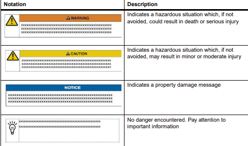
Notation Description
0x00000000 Typical notation for hexadecimal numbers (digits
are 0 through F), for example used for addresses
and offsets
0b0000 Same for binary numbers (digits are 0 and 1)
bold Used to emphasize a word
Screen Used for on-screen output and code related
elements or commands in body text
Courier + Bold Used to characterize user input and to separate it
from system output
Reference Used for references and for table and figure
descriptions
File > Exit Notation for selecting a submenu
<text> Notation for variables and keys
[text] Notation for software buttons to click on the screen
and parameter description
… Repeated item for example node 1, node 2, …,
node 12
.
.
.
Omission of information from example/command
that is not necessary at the time being
.. Ranges, for example: 0..4 means one of the
integers 0,1,2,3, and 4 (used in registers)
| Logical OR
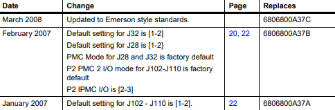
Summary of Changes
This manual has been revised and replaces all prior editions
Comments and Suggestions
We welcome and appreciate your comments on our documentation. We want to know what you
think about our manuals and how we can make them better.
Mail comments to us by filling out the following online form:
http://www.emersonnetworkpowerembeddedcomputing.com/ > Contact Us > Online Form
In “Area of Interest” select “Technical Documentation”. Be sure to include the title, part number,
and revision of the manual and tell us how you used it
Overview
This chapter contains the following information:
z Board and accessory preparation and installation instructions
z ESD precautionary notes
1.2 Introduction
The MVME5500 is a single-board computer based on the PowerPC MPC7457 processor and
the Marvell GT-64260B host bridge with a dual PCI interface and memory controller. On-board
payload includes two PMC slots, two SDRAM banks, an expansion connector for two additional
banks of SDRAM, 8MB boot Flash ROM, one 10/100/1000 Ethernet port, one 10/100 Ethernet
port, 32MB expansion Flash ROM, two serial ports, NVRAM and a real-time clock.
The MVME5500 interfaces to a VMEbus system via its P1 and P2 connectors and contains two
IEEE 1386.1 PCI mezzanine card (PMC) slots. The PMC slots are 64-bit and support both front
and rear I/O.
Additionally, the MVME5500 is user-configurable by setting on-board jumpers. Two I/O modes
are possible: PMC mode or SBC mode (also called 761 or IPMC mode). The SBC mode uses
the IPMC712 I/O PMC and the MVME712M transition module, or the IPMC761 I/O PMC and
the MVME761 transition module. The SBC mode is backwards compatible with the MVME761
transition module and the P2 adapter card (excluding PMC I/O routing) used on the MVME5100
product. This mode is accomplished by configuring the on-board jumpers and by attaching an
IPMC761 PMC in PMC slot 1. Secondary Ethernet is configured to the rear.
PMC mode is backwards compatible with the MVME5100 and is accomplished by configuring
the on-board jumpers.
1.3 Getting Started
This section provides an overview of the steps necessary to install and power up the
MVME5500 and a brief section on unpacking and ESD precautions.
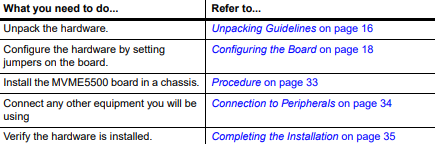
1.4 Overview of Startup Procedures
The following table lists the things you will need to do before you can use this board and tells
where to find the information you need to perform each step. Be sure to read this entire chapter,
including all Caution and Warning notes, before you begin.
1.5 Unpacking Guidelines
Unpack the equipment from the shipping carton. Refer to the packing list and verify that all items
are present. Save the packing material for storing and reshipping of equipment.
If the shipping carton is damaged upon receipt, request that the carrier’s agent be present
during the unpacking and inspection of the equipment.
Table 1-1 Startup Overview
ESD
Emerson strongly recommends that you use an antistatic wrist strap and a
conductive foam pad when installing or upgrading a system. Electronic components,
such as disk drives, computer boards, and memory modules can be extremely
sensitive to electrostatic discharge (ESD). After removing the component from its
protective wrapper or from the system, place the component flat on a grounded,
static-free surface (and, in the case of a board, component side up). Do not slide the
component over any surface.
If an ESD station is not available, you can avoid damage resulting from ESD by
wearing an antistatic wrist strap (available at electronics stores) that is attached to an
active electrical ground. Note that a system chassis may not be grounded if it is
unplugged.
Personal Injury or Death
Dangerous voltages, capable of causing death, are present in this equipment.
Use extreme caution when handling, testing, and adjusting.
Configuring the Hardware
This section discusses certain hardware and software tasks that may need to be performed
prior to installing the board in a chassis.
To produce the desired configuration and ensure proper operation of the MVME5500, you may
need to carry out certain hardware modifications before installing the module.
Most options on the MVME5500 are software configurable. Configuration changes are made
by setting bits in control registers after the board is installed in a system.
Jumpers and switches are used to control those options that are not software configurable.
These settings are described further on in this section. If you are resetting the board jumpers
or switches from their default settings, it is important to verify that all settings are reset properly.
Configuring the Board
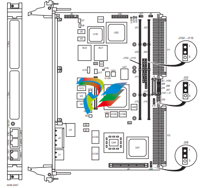
Figure 1-1 illustrates the placement of the jumpers, headers, switches, connectors, and various
other components on the MVME5500. There are several manually configurable headers and
switches on the MVME5500 and their settings are shown in Table 1-2. Each default setting is
enclosed in brackets. For pin assignments on the MVME5500, refer to Chapter 5, Connector
Pin Assignments.
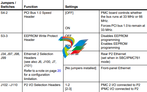
Table 1-2 MVME5500 Jumper Settings
Jumpers /
Switches Function Settings
J6, J100, J7,
J101
Ethernet 2 Selection
Headers
(see also J34, J97, J98,
J99)
Refer to the hint on page 7
for a configuration
limitation.
2-3 on all
[1-2 on all]
Rear P2 Ethernet (SBC mode)
Front-panel Ethernet
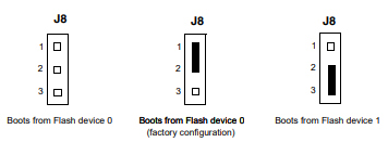
J8 Flash Boot Bank Select
Header
No jumper installed
[1-2]
2-3
Boots from Flash 0
Boots from Flash 0
Boots from Flash 1
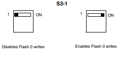
S3-1 Flash 0 Programming
Enable Header
OFF
[ON]
Disables Flash 0 writes
Enables Flash 0 writes
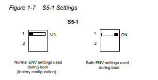
S5-1 Safe Start ENV Header [OFF]
ON
Normal ENV settings used
during boot
Safe ENV settings used during
boot
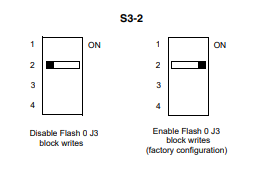
S3-2 Flash 0 Block Write
Protect Header
OFF
[ON]
Disables Flash 0 J3 block
writes
Enables Flash 0 J3 block writes
S3-4 Non-Standard Option
Header
[OFF] For factory use only
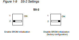
S5-2 SROM Initialization
Enable Switch
OFF
[ON]
Enables SROM initialization
Disables SROM initialization
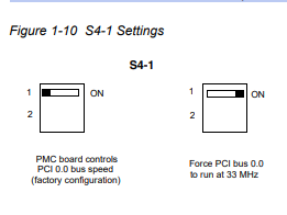
S4-1 PCI Bus 0.0 Speed
Header
[OFF]
ON
PMC board controls whether
the bus runs at 33 MHz or
66 MHz
Forces PCI bus 0.0 to remain at
33 MHz
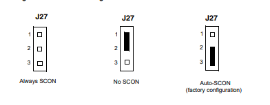
J27 VME SCON Select
Header
No jumper installed
1-2
[2-3]
Always SCON
No SCON
Auto-SCON
J28, J32 PMC/SBC Mode Selection
Headers
(set both jumpers)
Refer to page 7 for a
notice about configuring
for IPMC mode.
1-2 on both
2-3 on both
[1-2 on J28]
[2-3 on J32]
PMC mode
SBC/IPMC761 mode
SBC/IPMC712 mode
Table 1-2 MVME5500 Jumper Settings
The MVME5500 is factory tested and shipped with the configuration described in the following
section.
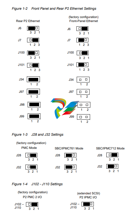
1.6.2 Ethernet 2, PMC/SBC Mode, and P2 I/O Selection Headers (J6,
J7, J28, J32, J34, J97 – J110)
All of the headers described below are used in conjunction with each other to select various
modes of operation for 10/100BaseT Ethernet, PMC/SBC mode, and P2 I/O mode.
1.6.2.1 Ethernet
Four 3-pin planar headers (J6, J7, J100, J101) and four 2-pin planar headers (J34, J97, J98,
J99) are for 10/100/BaseT Ethernet 2 selection.
Ethernet 1 is the Gigabit Ethernet port and is front panel only.
Figure 1-1 MVME5500 Board Layout
For J6, J100, J7 and J101, install jumpers across pins 2-3 on all four headers for rear P2 Ethernet. For front-panel Ethernet, install jumpers across pins 1-2 on all four headers. For J34, J97, J98 and J99, no jumpers are installed for front-panel Ethernet. For rear P2 Ethernet, install jumpers across pins 1-2 on all four headers when in SBC/IPMC761 mode. 1.6.2.2 PMC/SBC Mode Selection The MVME5500 is set at the factory for PMC mode. The SBC/IPMC761 mode should only be selected when using the IPMC761 module in conjunction with the MVME761 transition module.The PMC mode should be selected when using PMC modules with specific user I/O in conjunction with the corresponding transition module. PMC mode should also be selected when using PrPMC modules. Two 3-pin planar headers (J28, J32) control the supply of +/- 12 volts to the P2 connector; one or both of these voltages are required by the MVME712 or MVME761 module when operating in SBC mode. For PMC mode, jumpers are installed across pins 1-2 on both headers. For SBC/IPMC761 mode, install jumpers across pins 2-3 on both headers. For SBC/IPMC712 mode, install a jumper across pins 2-3 for J32 and install a jumper across pins 1-2 for J28. 1.6.2.3 P2 I/O Selection Nine 3-pin planar headers (J102 –J110) are for P2 I/O selection. Jumpers are installed across pins 1-2 on all nine headers when in PMC mode. Install jumpers across pins 2-3 on all nine headers when in SBC/IPMC761 or SBC/IPMC712 mode to connect the extended SCSI signals to P2. If the rear P2 Ethernet is selected by jumpers J6, J7, J100, and J101, the Ethernet signals also connect to PMC 1 user I/O connector J14. If a PMC card is plugged into PMC slot 1, there may be a conflict between the I/O from the PMC card and the rear Ethernet signals. This conflict does not occur with the IPMC761 or IPMC712 modules. Product Damage When J28 is configured for SBC/IPMC mode, –12V is supplied to P2 pin A30. If there is an incompatible board plugged into this P2 slot, damage may occur. When J32 is configured for SBC/IPMC mode, +12V is supplied to P2 pin C7. If there is an incompatible board plugged into this P2 slot, damage may occur.
Flash Boot Bank Select Header (J8)
A 3-pin planar header selects the boot Flash bank. No jumper or a jumper installed across pins
1-2 selects Flash 0 as the boot bank. A jumper installed across pins 2-3 selects Flash 1 as the
boot bank
Flash 0 Programming Enable Switch (S3-1)
This switch enables/disables programming of Flash 0 as a means of protecting the contents
from being corrupted. The switch set to OFF disables all Flash 0 programming. The switch set
to ON enables the programming, this is the factory setting.
Safe Start ENV Switch (S5-1)
This switch selects programmed or safe start ENV settings. When set to OFF, it indicates that
the programmed ENV settings should be used during boot. Set to ON indicates that the safe
ENV settings should be used.
Flash 0 Block Write Protect Switch (S3-2)
This switch supports the Intel J3 Flash family write protect feature. Set to OFF, it enables the
lock-down mechanism. Blocks locked down cannot be unlocked with the unlock command. The
switch must be set to ON in order to override the lock-down function and enable blocks to be
erased or programmed through software. Refer to the Intel J3 Flash data sheet, listed in
Appendix C, Related Documentation, for further details.
SROM Initialization Enable Switch (S5-2)
This switch enables/disables the GT-64260B SROM initialization. When set to 2, it enables the
GT-64260B device initialization via I2C SROM. Set to ON disables this initialization sequence.
SROM Initialization Enable Switch (S5-2)
This switch enables/disables the GT-64260B SROM initialization. When set to 2, it enables the
GT-64260B device initialization via I2C SROM. Set to ON disables this initialization sequence.
PCI Bus 0.0 Speed Switch (S4-1)
This switch can force PCI bus 0.0 to run at 33 MHz rather than the standard method of allowing
the PMC board to control whether the bus runs at 33 MHz or 66 MHz. Set to 1, it allows the
PMC board to choose the PCI 0.0 bus speed. Set to ON forces PCI bus 0.0 to run at 33 MHz.
9 VME SCON Select Header (J27)
A 3-pin planar header allows the choice for auto/enable/disable SCON VME configuration. A
jumper installed across pins 1-2 configures for SCON disabled. A jumper installed across pins
2-3 configures for auto SCON. No jumper installed configures for SCON always enabled.
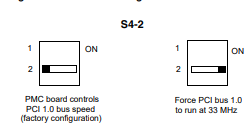
0 PCI Bus 1.0 Speed Switch (S4-2)
This switch can force PCI bus 1.0 to run at 33 MHz rather than the standard method of allowing
the PMC board to control whether the bus runs at 33 MHz or 66 MHz. Set to 1, it allows the
PMC board to choose the PCI 1.0 bus speed. Set to ON forces PCI bus 1.0 to run at 33 MHz.
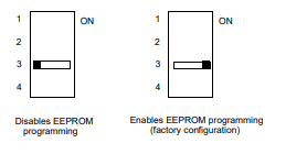
1 EEPROM Write Protect Switch (S3-3)
This switch enables/disables programming of the on-board EEPROMs as a means of protecting
the contents from being corrupted. Set to 1, it disables EEPROM programming by driving the
WP pin to a logic high. Set to ON to program any of the EEPROMs at addresses A0, A6, A8,
and/or AA.
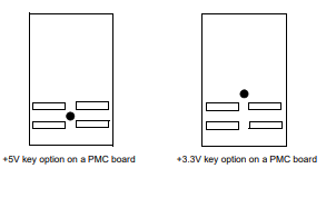
Setting the PMC Vio Keying Pin
Signalling voltage (Vio) is determined by the location of the PMC Vio keying pin. Each site can
be independently configured for either +5V or +3.3V signalling. The option selected can be
determined by observing the location of the Vio keying pin.
Installing the RAM5500 Module
Procedure
To upgrade or install a RAM5500 module, refer to and proceed as follows:
1. Attach an ESD strap to your wrist. Attach the other end of the ESD strap to the
chassis as a ground. The ESD strap must be secured to your wrist and to ground
throughout the procedure.
2. Perform an operating system shutdown. Turn the AC or DC power off and remove
the AC cord or DC power lines from the system. Remove the chassis or system
cover(s) as necessary for access to the VME boards.
3. Carefully remove the MVME5500 from its VME card slot and lay it flat, with
connectors P1 and P2 facing you.
4. Inspect the RAM5500 module that is being installed on the MVME5500 host board
to ensure that standoffs are installed in the four mounting holes on the module.
5. With standoffs installed in the four mounting holes on the RAM5500 module, align
the standoffs and the P1 connector on the module with the four holes and the P4
connector on the MVME5500 host board and press the two connectors together
until they are firmly seated in place.
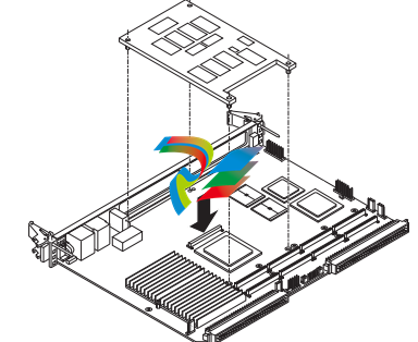
6. Turn the entire assembly over and fasten the four short Phillips screws to the
standoffs of the RAM5500.c
Leave a comment
Your email address will not be published. Required fields are marked *